- Home
- Products & Services
- Design Solutions
- High-speed Transmission
PRODUCTS & SERVICES
High-speed Transmission
Reducing loss and reflection is a key factor for GHz-speed transmission.
We implement high-speed transmission, taking the impact on board characteristics and design conditions into account.
Background
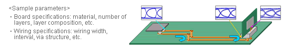
With GHz-speed printed boards, it is essential to select board specifications and wiring conditions with consideration for the transmission characteristics of the transmission channels (signal wires/vias). Additionally, the pattern layout itself (e.g. the way that wiring is drawn and how vias are created) affects the characteristics during board design. For this reason, the design must be made with an understanding of this impact.
Features
We support high-speed transmission printed boards by maximally combining transmission analysis, layout design, board materials, and manufacturing technologies.
Analysis services
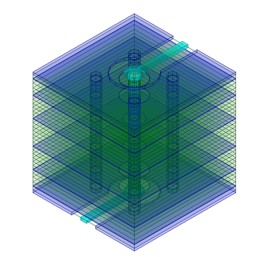
- 3D electromagnetic field analysis (channels, vias, connectors, etc.)
- High-accuracy simulation for high-frequency vias
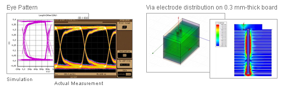
Realizes via characteristics compatible with high frequencies.
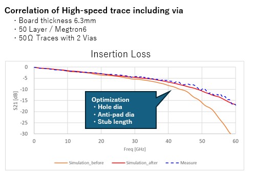
High-precision modeling technology helps control the via characteristics of multilayer PCBs, contributing to the development of high-speed transmission printed circuit boards and shortening development time. [Features]
- Supports high-accuracy simulation of 1.6Tbps class high-frequency vias
- 3D modeling technology that takes manufacturing processes into consideration
- Via characteristic impedance control correlated with actual measurements
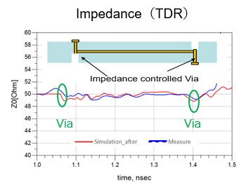
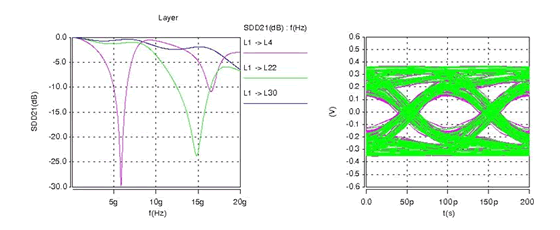
- S parameter analysis, eye pattern analysis, TDR analysis, etc.
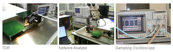
Measurement and evaluation
- Characteristic impedance
- Eye pattern
- S parameters (4 ports)
Sample analysis
- Related Products
- Related solutions
- Inquiry about Industries
- Inquiry from web: Inquiry form