- Home
- Products & Services
- Semiconductor Testing / ATE
PRODUCTS & SERVICES
Semiconductor Testing / ATE
Semiconductor technologies continue to advance. There is a need for high-precision processing technologies for multilayer/large testing boards to support larger wafers with large pin counts. There is also a need top-rate electrical characteristics, in order to support faster transmission signalling. High-precision/high-detail processing technologies are required to support decreasing package sizes.
We offer semiconductor testing boards, supporting from the background the reliable quality of continually evolving semiconductor devices.
Probe cards
- OKI Circuit Technology Technologies
- We offer high-precision/multilayer boards supporting high pin counts.
- We offer high-spectrum boards supporting high pin counts with narrow pitch (0.65 mm).
- We reduce development cycles through parallel, simultaneous design and our special production readiness.
- Product Specifications
- Layers: 4 to 40
- Aspect ratio: 21 (note: some variation in board thickness)
- Max. dimensions: 480 x 480 mm
- Board thickness: up to 6.3 mm
- Material: FR-4, FR-5 equivalent, polyimide
- Surface finish: electroless gold

Performance boards/DUT boards
- OKI Circuit Technology Technologies
- We offer high-precision/multilayer boards supporting high pin counts.
- We offer high-spectrum boards supporting narrow pin pitch (0.5 mm).
- We provide transmission-channel simulation technologies and high-precision control of characteristic impedance, supporting top-rated electrical characteristics through high-speed signal transmission.
- We reduce development cycles through parallel, simultaneous design and our special production readiness.
- Product Specifications
- Layers: 4 to 40
- Aspect ratio: 21 (note: some variation in board thickness)
- Max. dimensions: 488 x 630 mm
- Board thickness: up to 6.3 mm
- Material: FR-4, FR-5 equivalent, polyimide
- Structure: PTH, pad-on-via
- FBGAs supported to date: 0.5 mm, 0.65 mm, 0.8 mm
- Surface finish: electroless gold (up to 3 µm)

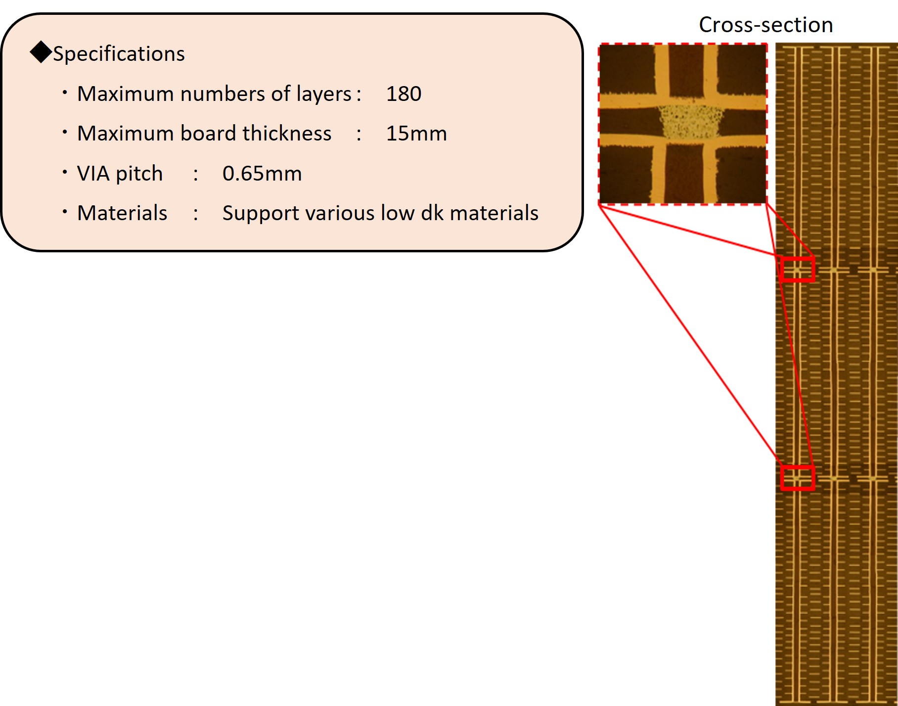
Printed Circuit Board using Sintering Paste for Via Bonding<180-layer 15mm thickness>
Realize ultra multilayer PCB (180 layers 15 thickness) by using conductive paste connection for Via bonding between substrate
- Features
- Realize ultra-high layer PCB by stacking and connecting multi-layer PCB (Connect vias on the surface)
- Support exceeding 7.6 thickness PCM while conventional manufacturing process had limitations in terms of drill bit length and production line
- By increasing board thickness, we can now handle more than 124 layers
- In addition to ultra-high thickness and ultra-high layers, it is possible to expand wiring area in conjunction with IVH
- Application example
- Semiconductor testing equipment Prove card
- Product overview and specifications
Burn-in boards
- OKI Circuit Technology Technologies
- We offer high-integration/large/multilayer boards supporting high pin counts (1,000-pin class).
- We offer high-precision large boards supporting narrow pin pitch (0.5 mm).
- Product Specifications
- Layers: 2 to 14
- Max. dimensions: 482 x 623 mm
- Board thickness: 1.6 mm+
- Material: FR-4, FR-5 equivalent
- Surface finish: HASL/electroless gold/OSP
- Socket pitch: 0.5 mm+
- Structure: PTH, pad-on-via

- Related Solutions
- Related Services
- Inquiry about Industries
- Inquiry from web: Inquiry form