Column
What Is a Printed Circuit Board?
An Introduction to PCB for Beginners: Explaining the Role, Types, and Manufacturing Process of PCBs
A term similar to “printed circuit board (PCB)” is “printed wiring board (PWB).” While “PWB” is the official term used in standards such as JIS, “PCB” is more commonly used in practice and in everyday language.
The Role of PCBs
The primary role of a PCB is to electrically connect electronic components. Circuit patterns on the board make it possible to miniaturize complex circuits and increase circuit density. PCBs also help secure and protect components, streamline assembly work, and improve mass-production efficiency. PCBs are used in a wide range of fields, including home appliances, communications equipment, and automobiles, and are indispensable to electronic devices. OKI Circuit Technology’s products are primarily used in industrial applications such as aerospace and defense, semiconductor testing equipment, and social infrastructure.
PCB Manufacturing Process
PCB Materials
The materials used in PCBs are a critical factor in determining board performance. Copper-clad laminate (CCL), the primary material for PCBs, typically consists of resin-impregnated glass cloth as the insulating layer and copper foil as the conductive layer. It offers excellent heat resistance, insulation, and mechanical strength. Copper foil, which has high electrical conductivity, is used for the conductor layers and is laminated onto the surface of the substrate material. In addition, when high-frequency characteristics are required, special materials such as PTFE are used. Selecting the optimal material according to the application and required performance is essential for manufacturing highly reliable PCBs. OKI Circuit Technology handles more than 20 types of materials and selects the most suitable material according to customer requirements and applications.
Inner Layer Process for PCBs
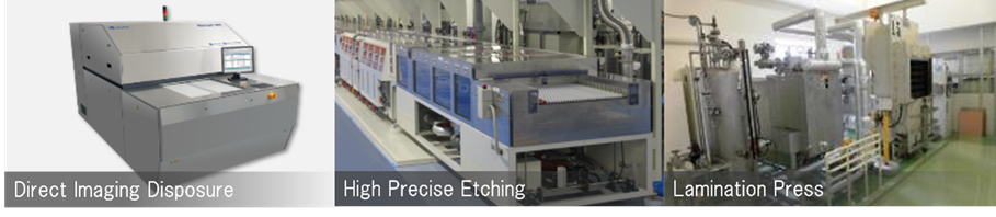
The inner layer process is a critical step in the manufacture of multilayer PCBs. First, photoresist is applied to the substrate material based on the design data. Next, a pattern is formed through exposure and development, and unwanted copper foil is removed by etching. This completes the inner-layer circuit. After that, multiple inner-layer boards are laminated and bonded together through heating and pressing. Because the inner layer process directly affects circuit precision and reliability, it requires a clean environment and advanced technical expertise. In today’s electronic devices, which are becoming increasingly dense and multifunctional, quality control in the inner layer process is extremely important.
Outer Layer Process for PCBs
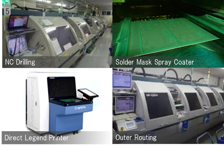
The outer layer process is a critical step that directly affects component mounting and circuit reliability. First, holes are drilled into the laminated board to form through-holes, and copper plating is applied to ensure electrical connectivity between the inner and outer layers. Next, photoresist is applied to the surface, and the pattern is exposed and developed according to the design. Afterward, unwanted copper foil is removed through etching to form the outer-layer circuit. Finally, surface treatments such as solder mask application and silk screening are applied, completing preparation for component mounting. Since the outer layer process significantly affects board quality, durability, and final product performance, it requires precise control and advanced technical expertise.
PCB Inspection Process
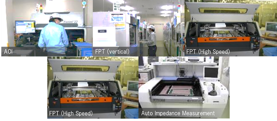
The inspection process is essential for ensuring product quality and reliability. It includes both intermediate inspection and final inspection. During intermediate inspection, patterns are checked using an automated optical inspection (AOI) system. During final inspection, electrical testing is performed using a flying probe tester to verify continuity, and a final visual inspection is conducted by human inspection or an automated visual inspection system to check the board surface for scratches, foreign matter, and missing patterns. At OKI Circuit Technology, all boards undergo 100% inspection to prevent defective products from reaching customers.
Types and Applications of PCBs
Through-Hole PCBs
Through-hole PCBs include single-sided boards, double-sided boards, and multilayer boards. Single-sided boards, also known as single-layer boards, are the simplest type of PCB, with circuit patterns formed on only one side of the board. Double-sided boards (2-layer boards) are PCBs with patterns formed on both sides, and they are chosen when the wiring cannot be accommodated on a single side. Because of their simple structure, they are low-cost and suitable for mass production.
Multilayer boards, on the other hand, are PCBs in which multiple wiring layers are stacked and electrically connected via through-holes that pass through the layers. This multilayer structure enables advanced electronic designs and high-density wiring. Multilayer through-hole PCBs also offer excellent signal transmission efficiency and noise suppression, and they are used in a wide range of fields, including personal computers, smartphones, communication devices, and automotive electronic control units. The ability to consistently manufacture through-hole PCBs—the most basic PCB structure—is an important foundation for ensuring the quality and reliability of more complex PCBs.
HDI PCBs
HDI PCBs are a type of multilayer PCB ideal for electronic devices that require high-density mounting. Unlike conventional multilayer through-hole PCBs, they feature a structure in which additional layers are built up on an already laminated board. By repeating the lamination process and using techniques such as laser processing, fine via holes are formed to connect the layers. This makes it possible to reduce trace widths and hole diameters to an extreme degree, enabling higher circuit density and smaller form factors. As a result, HDI PCBs are widely used in cutting-edge electronic devices such as smartphones, tablets, and wearable devices. Because this structure requires repeated lamination, it is essential to manufacture the board without misalignment between the inner layers and the added layers. HDI PCBs require advanced technical expertise and precise manufacturing processes, and they are a key foundational technology supporting the evolution of electronic devices.
Flex-Rigid PCBs
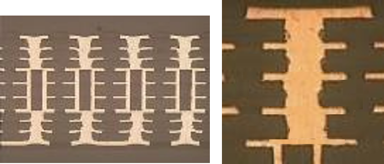
Flex-rigid PCBs are a composite type of PCB that integrates flexible and rigid substrates into a single board. The flexible portion is easy to bend, while the rigid portion offers superior strength and stability, making complex three-dimensional wiring and space-saving designs possible. This increases wiring flexibility inside electronic devices and can also reduce the number of components and assembly labor. Flex-rigid PCBs are widely used in fields that require lightweight, compact designs and high reliability, such as smartphones, digital cameras, medical devices, and automotive equipment. They also offer excellent durability and reliability, making them ideal for devices with many moving parts or products that require a high degree of design flexibility. However, the materials used in flexible sections present manufacturing challenges because of their elasticity and flexibility. Controlling expansion and contraction, which affect dimensional accuracy, and handling the boards carefully to prevent physical damage are both critical to quality.
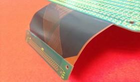
Distinctive PCBs from OKI Circuit Technology
Ultra-High-Multilayer PCBs
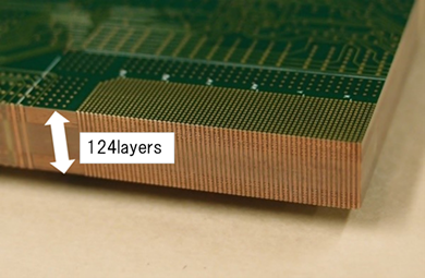
Ultra-high-multilayer PCBs are high-density, high-performance boards with multiple stacked wiring layers, and they are used mainly in semiconductor testing equipment. OKI Circuit Technology has successfully developed manufacturing technology for 7.6 mm-thick, 124-layer PCBs by developing ultra-thin materials, specialized tooling and handling methods, and a proprietary automated transport system for ultra-thin materials.
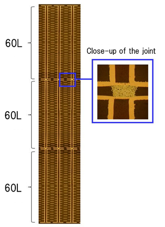
In addition, as part of our efforts in the area of thick PCBs, we have developed manufacturing technology for ultra-thick PCBs with board thicknesses of up to 15 mm, as well as conductive paste inter-board via connection technology (sintering paste connection technology) for stacking and connecting multiple multilayer boards. By combining these technologies, we have established proprietary PCB design and production technology that makes it possible to create a 15 mm-thick, 180-layer board by connecting three 60-layer PCBs.
PCBs for Space Applications
PCBs for space applications are highly reliable boards certified in accordance with the JAXA (Japan Aerospace Exploration Agency) specification “JAXA-QTS-2140.” OKI Circuit Technology is the only manufacturer in Japan to have obtained certification for all seven categories (Appendices A through H), and we are capable of supporting a wide range of space applications, including fine-pitch, flexible, flex-rigid, low-thermal-expansion, area-array package design, and high-speed signal boards. In addition, we offer a one-stop service ranging from artwork design to assembly. These boards deliver stable performance and durability even under the harsh conditions of space, which is why they have been adopted for satellites such as the H3 rocket and ALOS-4 (Daichi-4).
High-Speed, High-Frequency PCBs
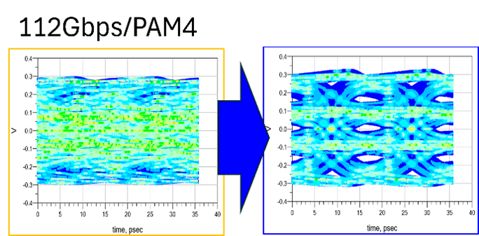
High-speed, high-frequency PCBs are widely used in high-end equipment such as communications infrastructure and semiconductor testing equipment. At OKI Circuit Technology, we have developed PCBs capable of supporting high-speed transmission rates of 100 Gbps or more by using low-loss materials and surface treatments that reduce the effects of skin effect, as well as build-up structures and back-drilling techniques. In addition, we can create custom structures that combine thick copper layers capable of handling the high currents required by high-power chips. To meet these demands, we provide integrated PCB simulation, design, and manufacturing services. These technologies are supported by high-precision simulations that show a strong correlation with actual measurements, helping to develop highly reliable and high-performance electronic devices.
High-Heat-Dissipation PCBs
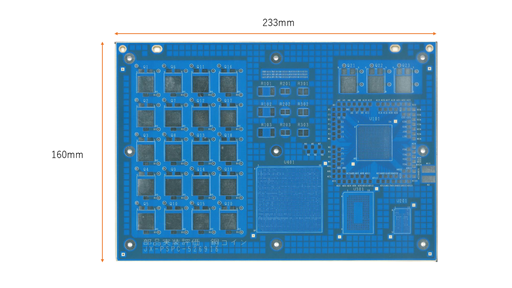
High-heat-dissipation PCBs require technologies that efficiently dissipate heat from heat-generating components. At OKI Circuit Technology, we achieve high heat dissipation through thick copper foil PCBs, metal-core PCBs, metal-base PCBs, and copper coin PCBs, which incorporate coin-shaped copper heat spreaders embedded within the PCB. The characteristics of each heat-dissipation structure are as follows:
- Thick copper foil PCBs: enable lateral heat dissipation and support high currents
- Metal-core PCBs: enable weight reduction and electromagnetic shielding
- Metal-base PCBs: allow direct heat dissipation from components
- Copper coin PCBs: enable localized heat dissipation and fine-pitch layout
These technologies help prevent performance degradation and failures caused by heat, contributing to improved product reliability. High-heat-dissipation PCBs are used in a wide range of electronic devices requiring thermal management and will continue to be a key technology in meeting demands for higher density and greater functionality.
Mixed-Thickness PCBs (Step Down PCBs)
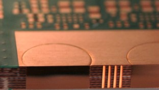
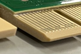
Mixed -thickness PCBs feature a special structure that allows the board thickness in the wiring section to be increased while maintaining the terminal section at the PCIe standard thickness of 1.57 mm. This makes it possible to support circuit designs requiring high multilayer counts and high density while still using existing PCIe connectors. While maintaining PCIe standards, this technology enables functional expansion of the entire board and improves reliability through the integration of the connector section and the wiring section. OKI Circuit Technology’s manufacturing technology for mixed-thickness PCBs is an advanced board technology that makes it possible to satisfy connector standards and high-layer-count designs at the same time, meeting the needs of a wide range of electronic devices.
Summary
PCBs are a critical technological foundation for electronic devices. OKI Circuit Technology plays an active role in fields that demand high technical expertise and consistent quality, such as semiconductors, aerospace and defense, telecommunications equipment, measuring instruments, and social infrastructure. Going forward, we will continue to innovate while meeting our customers’ diverse needs, and we will actively work to develop higher-performance, higher-quality PCBs
Contact Us
- Inquiry about Industries
- Inquiry from web: Inquiry form