Column
Effective Heat Dissipation:
OKI Circuit Technology’s Thermal Management Solutions
With high-density mounting and higher power output now standard, thermal management in printed circuit boards (PCBs) is crucial for optimal performance, reliability, and longevity. To address hot spots and create efficient thermal pathways, it’s vital to optimize materials, layer configurations, copper thickness, and overall structure.
In this column, we discuss the significance of thermal design for PCBs, present essential strategies, and highlight OKI Circuit Technology’s cutting-edge solutions—including our unique copper coin technology.
Why Is Thermal Design Crucial for PCBs?
Without proper heat diffusion and transfer by the PCB, both its performance and reliability are compromised. First, let’s outline the increase in heat-generating components, the trend toward high-density mounting, and the specific failures that heat can cause.
Trends in Increasing Heat Sources and High-Density Mounting
The number of heat-generating components mounted on PCBs—such as SoCs, GPUs, and RF/5G-related devices—is steadily increasing. At the same time, devices are continuously being made smaller, thinner, and capable of handling higher currents, making high-density mounting on limited PCB space a common necessity.
As a result, traditional methods for thermal management—like relying on large heatsinks or fans—have become less feasible. Now, the PCB itself is required to function as a key part of the overall thermal management system, diffusing and transferring heat effectively. Partial temperature rises often occur directly beneath high-current components and power device pads. Additionally, as PCBs become increasingly multilayered, heat dissipation pathways grow more complex.
It is becoming increasingly important to efficiently transfer heat from heat-generating components through inner copper planes and ultimately out to the chassis.
Let’s briefly review the three mechanisms of heat transfer:
| 1:Conduction | Conduction is the phenomenon where heat moves through solid chassis In PCBs, copper traces, vias, and copper coins facilitate rapid diffusion and transfer of heat. |
|---|---|
| 2:Convection | Thermal convection refers to the phenomenon where heat is carried away by air or cooling airflow, enabling the dissipation of heat from the PCB surface or heat sinks to the surrounding space. |
| 3:Radiation | Radiation is the phenomenon in which thermal energy is transmitted as electromagnetic waves, allowing direct transfer even without the presence of air. |
In practice, thermal management is optimized by using conduction to spread hotspots within the PCB, and by using convection and radiation to release heat from the PCB’s surface into the environment.
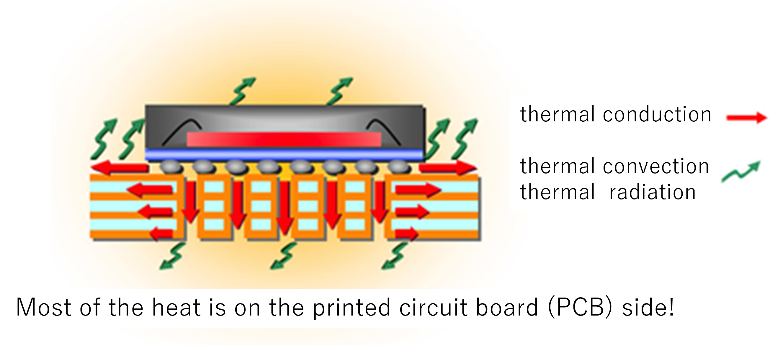
Figure 1:Mechanism of heat transfer
Issues Caused by Heat and Their Impact on Product Performance
Heat does more than simply raise temperatures—it accelerates various failure mechanisms. For example, differences in thermal expansion between materials during temperature cycling can lead to cracks in solder joints, particularly beneath BGAs or large-area pads, which can gradually progress and result in electrical contact failures.
Furthermore, residual stress within the PCB can cause warping, and even minor deformations after assembly may affect solder joint reliability and mechanical strength, which leads directly to issues such as inconsistent performance or shortened product life.
Incorporating thermal design and validation from the earliest stages of development is the most effective way to minimize post-production defects and warranty costs.
Key Thermal Management Strategies for PCBs
When planning thermal management for a PCB, it is essential to consider both how heat spreads within the PCB and the pathways for heat dissipation to the exterior. Begin by ensuring efficient in-plane heat diffusion, and then, as needed, strengthen out-of-plane heat conduction to direct heat away from the PCB.
In this section, we provide key points on the following methods: utilizing copper-based or thick-copper PCBs, designing thermal vias and heat-dissipating pads, and employing metal-core PCBs for heat dissipation.
Copper-Based and Thick Copper PCBs
Copper has excellent thermal conductivity. Increasing both the thickness and the area of copper layers enhances in-plane heat diffusion, making it easier to lower the temperature of hotspots. In particular, internal power and ground planes serve as key structures to absorb and spread heat directly from heat sources.
However, the use of thick copper requires careful manufacturing considerations. Forming fine pitches becomes more difficult, imposing constraints on trace width and spacing. At the design stage, it is essential to balance electrical and thermal requirements, while also optimizing layer configuration and dimensional tolerances to account for manufacturing variability.

Figure 2:Temperature distribution comparison by copper thickness
Designing Thermal Vias and Heat-Dissipating Pads
Thermal vias placed directly beneath thermal pads are highly effective for transferring heat from heat-generating components to the inner or bottom copper layers. These vias conduct heat away from device pads to larger copper areas or, through thermal conductive sheets, to heatsinks and chassis.
In the design process, via diameter and pitch should be optimized based on the recommended device specifications and manufacturing tolerances. It is also important to properly set pad diameter and anti-pad area, considering drill deviation and resist misalignment.
Adding more thermal vias improves heat conduction; however, it can also impact electrical return paths and impedance. It’s crucial to balance thermal and electrical requirements, and carefully fine-tune via placement, layer structures, and via design.
Adoption of Metal-Core PCBs for Heat Dissipation
Metal-core PCBs, which feature stacked aluminum or copper cores, enable rapid heat dissipation due to the high thermal conductivity of the metal core. Additional advantages include enhanced mechanical strength, reduced weight, and electromagnetic shielding provided by the metal layer.
However, these PCBs come with certain limitations: multilayering and fine-trace patterning are more difficult, resulting in reduced design flexibility. Moreover, differences in the coefficients of thermal expansion between the metal core and other PCB materials can lead to mechanical stresses, which should be considered in the design.
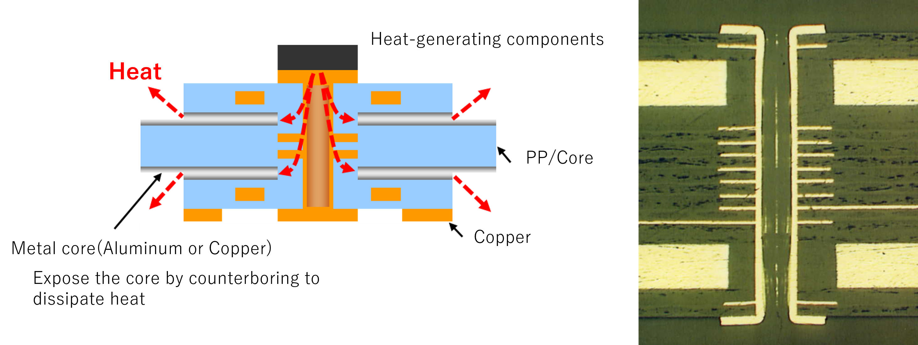
Figure 3:Example Structure of Metal-Core PCB
OKI Circuit Technology’s Thermal Management Solutions
We at OKI identify thermal bottlenecks through simulation analysis and propose optimized solutions—including thick copper layers, thermal via designs, and copper coin technology—to enhance heat dissipation.
Efficient Heat Dissipation Solutions with Copper Coin Technology
Copper coin technology involves embedding copper blocks directly beneath heat sources, forming a “short and thick” thermal path that conducts heat efficiently from the source to the chassis or heatsink. Compared to using multiple thermal vias, copper coins offer a much larger cross-sectional area and fewer interfaces, significantly reducing thermal resistance.
Copper coins can be selectively placed only where needed and are also compatible with fine-pitch wiring and narrow-pitch BGAs, enhancing design flexibility. Through thermal simulations that consider layer configuration and surrounding planes, we determine the optimal coin size and assess the temperature reduction effect. Copper coins are especially effective in areas with spot heat generation or where direct heat transfer to the chassis is feasible.
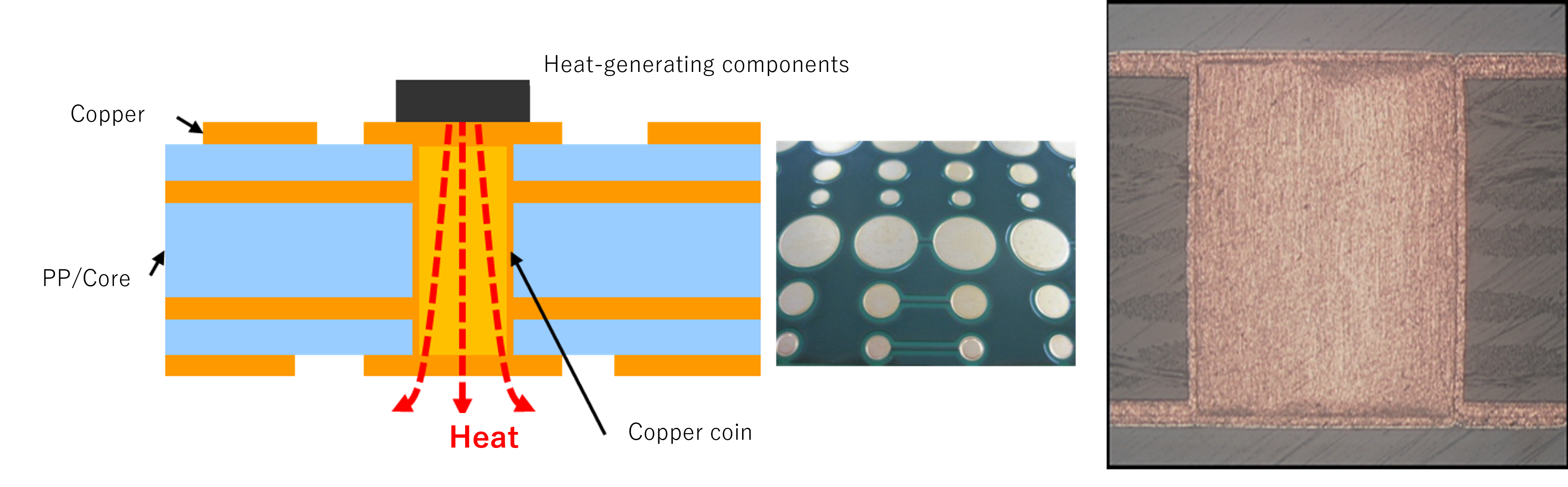
Figure 4:Cross-sectional structure of copper coin and heat transfer path to chassis
For applications used in space, where natural convection in a vacuum is not possible, heat dissipation depends almost entirely on conduction through the PCB or chassis, as well as radiation. Therefore, forming “short and thick” conduction paths from heat sources to the chassis, panel, or radiator using copper coins offers a clear advantage. We have extensive experience with space-grade PCBs and can assist in designing conduction-focused thermal solutions—such as optimizing copper thickness, coin dimensions, and placement—for efficient heat transfer.
Thermal Simulation for Multilayer PCBs
From the earliest stages of development, OKI applies thermal simulations to visualize hotspot locations and temperature distributions. Based on these results, we compare multiple thermal management options—including thick copper, thermal vias, copper coins, and chassis connections. Heat generation by components is modeled using datasheet specifications and actual usage conditions, while environmental factors are also considered. We systematically vary layer configurations, copper density, and via placement to evaluate temperature profiles and cooling performance.
In particular, we thoroughly evaluate the effectiveness of copper coins compared to high-density thermal via arrays in the early stages, and propose solutions that reliably achieve the target temperatures. This front-loading enables the minimization of rework in the later development stages, optimizing both the development timeline and overall cost.
Conclusion
With the trends toward high-density mounting and higher power output, it is essential to design PCBs as effective heat diffusers and conductors. Optimal thermal management employs a combination of conduction, convection, and radiation—spreading heat away from hotspots within the PCB and dissipating it to the chassis.
Temperature increases can lead to issues such as solder joint cracking and PCB warping. Therefore, it’s crucial to incorporate thermal design and verification from the earliest development stages. Structural options—such as thick copper, thermal vias, metal-core, and copper coin solutions—should be matched to the specific thermal requirements of the application.
At OKI, we visualize thermal bottlenecks through simulation and propose solutions such as optimizing copper thickness (105–240 µm), via placement, and designing “short and thick” copper coin pathways. These approaches support you in achieving target temperatures and improving development efficiency.
Contact Us
For inquiries about thermal management challenges or the feasibility of implementing specific copper thickness, copper coins, or via specifications, please contact us via our inquiry form. If you can provide details such as your application, environmental conditions, target temperature, and chassis specifications, we will be happy to propose an evaluation approach and provide a quotation.
- Inquiry about Industries
- Inquiry from web: Inquiry form