- Home
- Products & Services
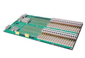
- High-speed high-frequency PCB
PRODUCTS & SERVICES
High-speed high-frequency PCB
Improvement of transmission characteristics
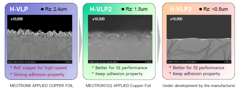
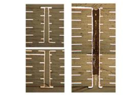
Improvement of conductor loss due to roughness of copper foil surface
Since the high-frequency signal (current) flows through the conductor surface by the epidermis effect, the smoothness of the conductor surface is the key.
Improvement of transmission characteristics
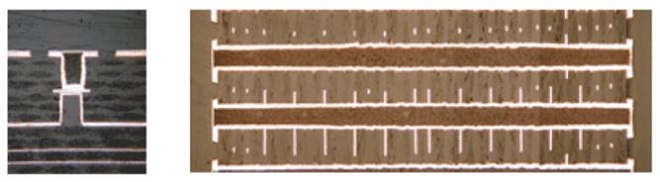
Improvement of conductor loss by surface treatment method
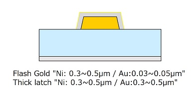
Conductor loss differs depending on the surface treatment. Especially in the high-frequency band, the influence of surface treatment is large due to the epidermis effect.
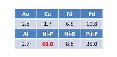
Electric resistance(uΩ・cm)
Comparison processing thickness
- Electroless Ni/Thickness Au …"Ni: 5.00μ/Au:0.30μ"
- Ni/Pd/Au …"Ni: 5.00μ/Pd:0.10μ/Au:0.30μ"
- Pd/Au (prototype): "Pd: 0.15μ/Au:0.03μ"
- Flash gold: "Ni: 3.00μ/Au: 0.03μ"
- Au/Pd/Au …"Au0.02μ/Pd: 0.10μ/Au:0.08μ"
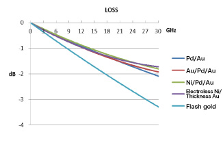
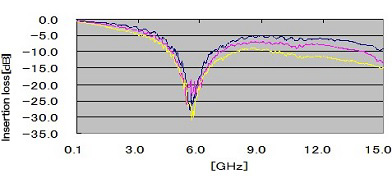
Material: R-5775N (MEGTRON6N)Line length: 54.1mm
Improvement of transmission characteristics
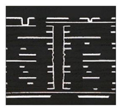
Improving VIA Loss by Backdrilling
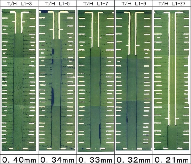
Before processing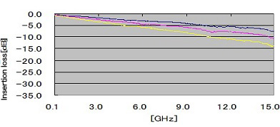
After processing
Improvement of transmission characteristics
Loss improvement by low dielectric material and low dielectric tangent material
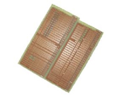
IVH(Interstitial Via Hole)board
- Holding Technology
- Board type: BWB for press-fit, IC tester board, etc.
- Layer: upto 50
- Size: 670 x 570 mm max. Thickness: 6.3 mm max.
- Characteristic impedance control: +/-5%
- Material: FR-4, FR-5, BT, Polyimide, Low dk
- Product Specifications
- Layer: 20
- Structure: IVH, 10+10
- Board thickness: 3.2 mm (.126")
- Board size: 340 x 366.67 mm (13.39" x 14.44")
- Line width/space OL: 0.127/0.110 mm (.005/.0043") IL 0.1/0.114 mm (.004/.0045")
- Min. hole size (drill size) PTH: 0.35 mm (.0014"). IVH 0.25 mm (.001")
- Surface finish: HASL
- Material High Tg: FR-4
- Characteristic impedance: Single-end 50 ohm +/-10%, differential 90 ohm +/-10%
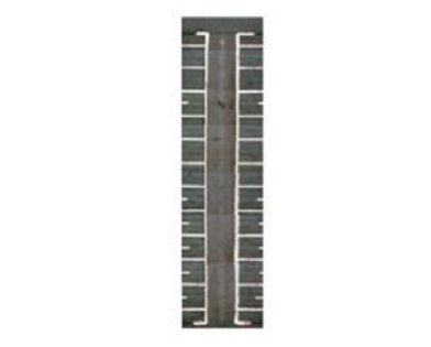
PAD on VIA board
- OKI Circuit Technology Technologies
- Capability of Resin-Filling
- OKI Circuit Technology Technologies
-
- Capability of Resin-Filling
- Product Specifications
-
- Board size: 590 x 480 mm max.
- Board thickness: 0.6 to 6.3 mm
- Hole size: 0.35 mm/6.3 mm thick; 0.2 mm/3.5 mm thick
- Pad-on-via: OK
- Micro-via (bottomed) filling: 0.13 mm
Hiper Via board
- Product Specifications
-
- Layers: 16
- Laser micro vias: L1-2, L2-3
- Board thickness: 2.1 mm (.083")
- Board size: 235 x 415 mm (9.25 x 16.34")
- Line width/space: 0.10/0.10 mm (.004/.004")
- Min. hole size (drill size): 0.3 mm (.0012")
- Surface finish: Immersion silver
- Material: High Tg FR-4
- Characteristic impedance: 55 ohm +/-10%
Back-drill board
- Product Specifications
-
- Layers: 26
- Laser micro vias: L1-2, L2-3
- Board thickness: 2.1 mm (.083")
- Board size: 235 x 415 mm (9.25 x 16.34")
- Line width/space: 0.10/0.10 mm (.004/.004")
- Min. hole size (drill size): 0.3 mm (.0012")
- Surface finish: Immersion silver
- Material: High Tg FR-4
- Characteristic impedance: 55 ohm +/-10%
- Inquiry about Industries
- Inquiry from web: Inquiry form