Column
What is Impedance?
Impedance control for PCB Design and Manufacturing
Impedance control is a crucial technology for high-performance, high-quality printed circuit boards. This technology optimizes the electrical performance by maintaining signal quality and suppressing reflection and interference.
In recent years, This importance has been increasing day by day in electronic products which requiring high-speed and high-capacity data transfer, such as communications, computing, and IoT devices.
In this article, we will provide a detailed explanation, covering from the basics of impedance control to the latest solutions and trends.
What is Impedance?
Impedance is the concept of resistance in electrical circuits. While it's represented by a simple resistance value in DC circuits, AC circuits require the more complex concept of impedance.
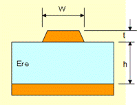
Impedance is also a crucial indicator that represents the relation between voltage and current in AC circuits. The trace) impedance on printed circuit boards is determined by the cross-sectional dimensions of the wiring (width/thickness of trace, distance from reference plane) and material properties (dielectric constant).
Overview of Impedance Control
Impedance control refers to the technology of designing, manufacturing, and managing PCB signal traces to maintain consistent impedance. This technology is essential for ensuring high-frequency signal transmission quality. It plays a particularly crucial role in high-speed digital circuit and wireless communication equipment design.
Typical impedance control considers manufacturing variations, with tolerances such as ±10%
Importance of Impedance Control
Proper impedance control prevents signal reflection and distortion, enabling high-quality signal transmission. This significantly improves the performance and reliability of high-speed and high-frequency circuits.
For example, high-speed data transfer equipment such as servers and 5G communication devices. In such equipment, impedance control is a crucial factor that determines product performance and communication quality.
Role of PCB Design
Impedance control must be implemented from the PCB design stage and contributes to ensuring signal quality and reducing EMI (electromagnetic interference). Precise impedance control requires appropriate conditions and compatible design at the design stage.
Particularly in high-speed digital circuits and RF (radio frequency) circuits, design quality affects performance. Proper PCB design and impedance control maintain signal integrity and optimize overall circuit performance.
Reasons for Impedance Control
Improving Signal Quality
Impedance control maintains high-quality signal propagation from driver to receiver and ensures communication integrity. These are essential for SI (signal integrity) as they help reduce jitter and noise.
For example, in high-speed serial communication, data must be transmitted and received with precise timing. Proper impedance control ensures signal quality.
Reduction of Reflection and Interference
Signal reflection causes waveform distortion and cause communication errors. Impedance control can minimize these reflections.
Additionally, controlling the distance between adjacent signals helps reduce signal interference such as crosstalk. This is particularly important in modern PCB design where high-density mounting is required.

Importance in High-Speed Digital Circuits
Maintaining signal quality is crucial in high-speed signal transmission. Proper impedance control is able to reduce bit error rates and improve communication reliability.
For example, PCBs for high-speed communication exceeding 25Gbps require more precise impedance control. Control tolerances can become stricter, changing from ±10% to ±5% in some cases.
Theory and Practice of Impedance Matching
Concept of Impedance Matching
Impedance matching is the concept of aligning the impedance of the signal source, transmission line, and load. This minimizes overall system reflection, reduces energy loss from reflection, and enables maximum power transfer.
For example, in a 50Ω system, circuit design and PCB design are performed so that the signal source, transmission line, and load all have 50Ω impedance.
- Case 1: Transmission line 50Ω, load 75Ω

Part of the flow is reversed → Signal is reflecting at the point of impedance change.
- Case 2: Transmission line 50Ω, load 50Ω

No reverse flow → No reflection due to impedance matching.
Effects of Poor Matching
Insufficient matching causes waveform distortion due to signal reflection. This leads to bit errors in digital circuits and degradation of signal-to-noise ratio (S/N ratio) in analog circuits.
It also causes power loss and signal strength reduction, so caution is necessary.
Effective Matching Techniques
Effective matching requires both circuit design approaches, such as proper selection of termination resistors, and PCB design with appropriate component placement and wiring. It's also an effective method for designing and implementing impedance transformation circuits in RF circuits.
For example, using broadband matching circuits can achieve good matching across a wide frequency range.
Methods of Impedance Adjustment
Importance of Stack up Design
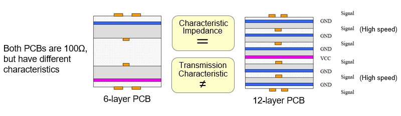
In multilayer PCBs, stack up (layer configuration) design that considers the impedance of each layer is crucial. This is because the direction changes significantly depending on how many signal layers require impedance control, how many power and ground planes are needed, and how much board thickness can be tolerated.
In recent high-speed transmission boards, ensuring power quality is equally important, and proper placement of power planes and ground planes significantly affects the operational stability of the entire board. For example, placing ground layers above and below high-speed signal layers improves signal quality from the perspective of impedance and return path.
Furthermore, because the set trace width changes depending on the layer configuration and interlayer thickness settings, even with the same differential 100Ω, characteristics including losses are not necessarily identical.
Optimization of Trace Width
There is a close relationship between impedance and trace width. Impedance can be controlled by adjusting the trace width.
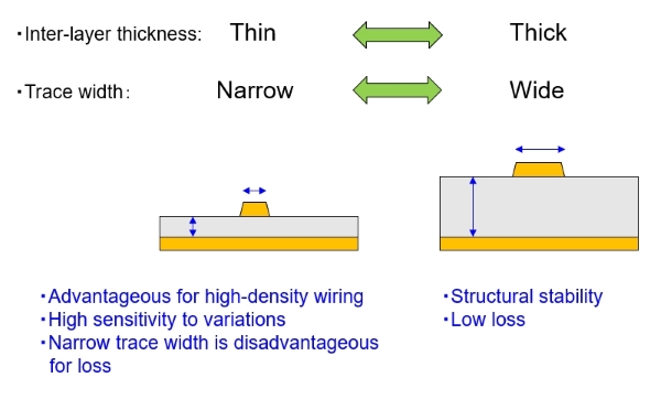
For example, in microstrip line structures, widening the trace width decreases impedance, while narrowing it increases impedance. For PCBs requiring high-density wiring, it's advantageous to set thinner trace widths considering wiring capacity.
However, thin conductor widths in high-speed signals lead to increased conductor loss. Therefore, when prioritizing characteristics, it's preferable to set wider signal trace widths.
Adjustment of Dielectric Thickness
Dielectric thickness also significantly affects impedance control. Desired impedance can be achieved through the selection of board materials and optimization of dielectric thickness.
Since dielectric thickness and trace width are related parameters, careful selection is necessary. For example, even when setting the same 50Ω, the trace width becomes thinner with thinner dielectric thickness and wider with thicker dielectric thickness.
Additionally, dielectric thickness relates to the degree of crosstalk influence between adjacent traces:
- With thick dielectric, the reference ground plane becomes more distant
- When signals are placed close together, signal coupling increases, leading to increased crosstalk
This means wider trace spacing is needed compared to cases with thin dielectric thickness, making design more challenging for boards requiring high-density design.
Impedance Calculation and Measurement
Calculation Formulas and Simulation Tools
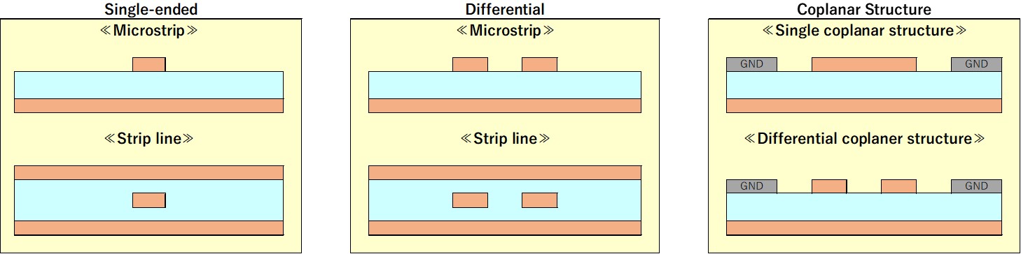
There are many types of impedance control structures:
- Microstrip line
- Strip line
- Single-ended
- Differential (differential signal)
- Coplanar structure
Therefore, various calculation formulas exist for impedance calculation. More precise calculations are possible using electromagnetic field simulation tools.
Our company proposes optimal conditions according to customer requirements using our proprietary calculation formulas based on years of factory experience and high-precision simulation technology.
Impedance Measurement Method
Time Domain Reflectometry (TDR) is a common method for measuring and evaluating impedance in printed circuit boards. With TDR, impedance can be confirmed on a time axis, allowing visual understanding of impedance values at any position.
Since TDR applies a step pulse and measures its response, the rise time (Tr) of the step pulse determines the measurement resolution. Our company performs high-precision impedance measurements using various TDR and automatic measuring instruments according to customer requirements.
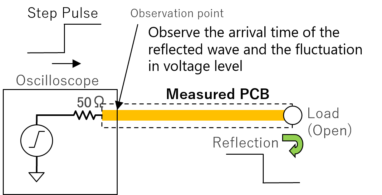
Step Pulse
Rise Time(tr)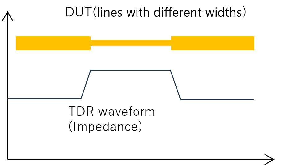
TDR measurement example
Practical Tips for Impedance Control
Design Considerations at PCB Design Stage
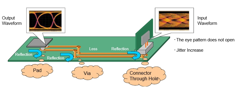
In PCBs requiring impedance control, wiring layout design is crucial. Particularly for high-speed signals, design techniques are required to minimize impedance changes in the relationship between signal wiring and ground planes serving as reference planes, as well as vias and component pads that are part of the transmission path.
Our company achieves optimal layout design utilizing years of experience and the latest CAD/CAE design tools. Specifically, it's important to determine impedance matching conditions for component pads and vias through simulation at the initial PCB design stage and perform layout design based on these conditions.
Finally, we verify whether the impedance meets expected conditions by simulating the completed CAD wiring data.
Manufacturing Process Control Points
PCB impedance management requires control of manufacturing precision and variations, as impedance changes with signal trace width and dielectric thickness.
Strict quality control throughout the manufacturing process - including etching and plating processes for signal trace width and lamination processes for dielectric thickness - achieves impedance within specified tolerances.
Latest Trends and Challenges
Response to High-Frequency and High-Speed Signals
PCBs for higher frequency applications such as 5G communications and millimeter waves are increasing. Impedance control in these high-frequency regions requires new technologies and knowledge.
Particularly for high-frequency applications, there's growing demand for via impedance control in addition to traditional wiring impedance control.
Targeted characteristics can be achieved through electromagnetic field analysis simulation, manufacturing variation control, and post-manufacturing board characteristic evaluation. Our company maintains cutting-edge technical knowledge and possesses design and manufacturing capabilities for next-generation high-speed interfaces.
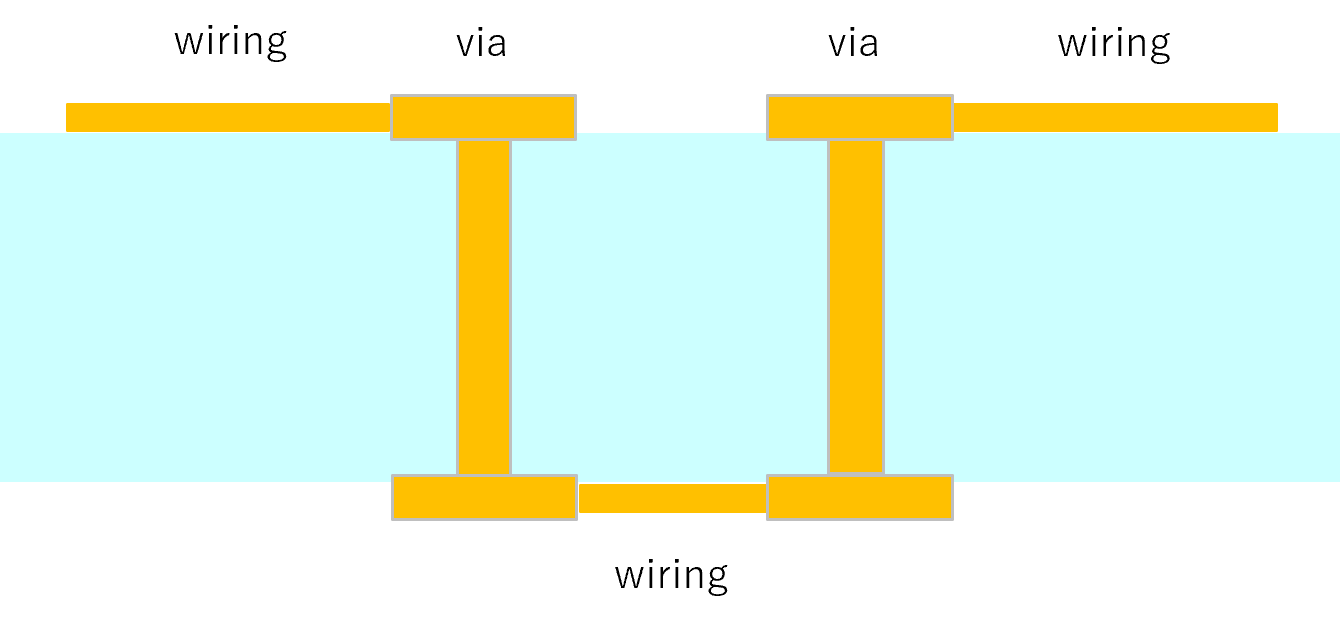
Wiring and Via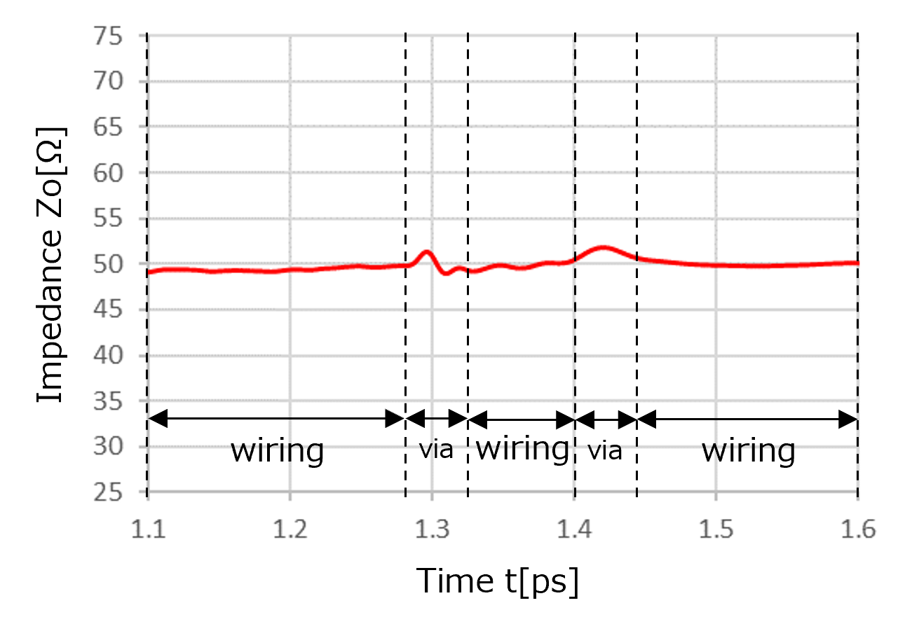
TDR waveform
Impedance Control in Fine Wiring
New challenges are arising in impedance control with wiring miniaturization, as variations in trace width that were previously acceptable now result in significant impedance changes.
Many cases require balancing high-density mounting technology with impedance control. We actively address these challenges through the introduction of latest etching lines and surface treatments that suppress roughness affecting conductor surface treatment.
Conclusion
Impedance control is an essential technology in high-performance, high-quality PCBs where characteristics are crucial. Our company provides optimal design and manufacturing solutions for various customer needs, leveraging years of experience and advanced technical capabilities.
We will continue technological innovation and lead next-generation PCB technology. For high-quality and reliable PCBs, please contact OKI Circuit Technology Corporation.
- Inquiry about Industries
- Inquiry from web: Inquiry form